martes, 18 de junio de 2013

RV: Nanoparticle opens the door to clean-energy alternatives

Fuente: Penn State News - Research
Expuesto el: martes, 18 de junio de 2013 11:21
Autor: Penn State News - Research
Asunto: Nanoparticle opens the door to clean-energy alternatives


UNIVERSITY PARK, Pa. -- Cheaper clean-energy technologies could be made possible thanks to a new discovery. Research team members led by Raymond Schaak, a professor of chemistry at Penn State, have found that an important chemical reaction that generates hydrogen from water is effectively triggered -- or catalyzed -- by a nanoparticle made of nickel and phosphorus, two inexpensive elements that are abundant on Earth. The results of the research will be published in the Journal of the American Chemical Society. More details and two photos are online at http://science.psu.edu/news-and-events/2013-news/Schaak6-2013.

Schaak explained that the purpose of this nanoparticle is to help produce hydrogen from water -- a process that is important for many energy-production technologies including fuel cells and solar cells. "Water is an ideal fuel, because it is cheap and abundant, but we need to be able to extract hydrogen from it," Schaak said. Hydrogen has a high energy density and is a great energy carrier, Schaak explained, but it requires energy to produce.

To make its production practical, scientists have been hunting for a way to trigger the required chemical reactions with an inexpensive catalyst. Platinum works, but it is expensive and relatively rare, so Schaak and his team have been searching for alternative materials. "There were some predictions that nickel phosphide might be a good candidate, and we already had been working with nickel phosphide nanoparticles for several years," Schaak said. "It turns out that nanoparticles of nickel phosphide are indeed active for producing hydrogen and are comparable to the best known alternatives to platinum."

Hydrogen gas bubbling off of the surface of a nickel phosphide crystal. A team led by Raymond Schaak of Penn State is studying nanoparticles made from nickel phosphide as a means to create cleaner energy technologies.

Image: Eric Popczun

To create the nickel phosphide nanoparticles, team members began with metal salts that are commercially available. They then dissolved these salts in solvents, added other chemical ingredients, and heated the solution to allow the nanoparticles to form. The researchers were able to create a nanoparticle that was quasi-spherical -- not a perfect sphere, but spherical with many flat, exposed edges. "The small size of the nanoparticles creates a high surface area, and the exposed edges means that a large number of sites are available to catalyze the chemical reaction that produces hydrogen," Schaak explained.

Team members at the California Institute of Technology then tested the nanoparticles' performance in catalyzing the necessary chemical reactions. They found that, not only were the chemical reactions happening as they had hoped, they also were happening with a high degree of efficacy.

"The goal now is to further improve the performance of these nanoparticles and to understand what makes them function the way they do," Schaak said. "Our team members believe that our success with nickel phosphide can pave the way toward the discovery of other new catalysts that also are comprised of Earth-abundant materials. Insights from this discovery may lead to even better catalysts in the future."

In addition to Schaak and Lewis, other researchers who contributed to this study include Eric J. Popczun, Carlos G. Read, Adam J. Biacchi and Alex M. Wiltrout from Penn State; and James R. McKone from the California Institute of Technology.

The research was funded by the U.S. National Science Foundation and the U.S. Department of Energy. The team has filed a patent application.


Ver artículo...

domingo, 16 de junio de 2013

RV: Unzipped nanotubes unlock potential for batteries

Fuente: Rice University News & Media » Current News
Expuesto el: jueves, 13 de junio de 2013 20:48
Autor: Mike Williams
Asunto: Unzipped nanotubes unlock potential for batteries


Researchers at Rice University have come up with a new way to boost the efficiency of the ubiquitous lithium ion (LI) battery by employing ribbons of graphene that start as carbon nanotubes.

Graphene nanoribbons split from nanotubes in a process created at Rice University are now being used to improve the performance of lithium ion batteries. The nanoribbons in a solution with tin oxide have more than double the capacity for lithium than standard graphene anodes in current commercial batteries. Image courtesy of the Tour Group

Proof-of-concept anodes — the part of the battery that stores lithium ions — built with graphene nanoribbons (GNRs) and tin oxide showed an initial capacity better than the theoretical capacity of tin oxide alone, according to Rice chemist James Tour. After 50 charge-discharge cycles, the test units retained a capacity that was still more than double that of the graphite currently used for LI battery anodes.

The research appeared this week in the American Chemical Society journal ACS Nano­­.

Better batteries are greatly desired by everyone who carries a cellphone or computer or drives an electric car. The Rice team sees the potential for GNRs to contribute to their development.

Tour and his colleagues developed a method for unzipping nanotubes into GNRs, revealed in a 2009 cover story in Nature. Since then, the researchers have figured out how to make graphene nanoribbons in bulk and are moving toward commercial applications. One area ripe for improvement is the humble battery. In an increasingly mobile world, battery capacity is becoming a bottleneck that generally limits devices to less than a day’s worth of use.

Islands of tin oxide ride alongside a graphene nanoribbon (at top) in a slurry used in anodes for lithium ion batteries. The 10-nanometer tin oxide particles are kept separated by the nanoribbons, which are created by splitting multiwalled carbon nanotubes. Image courtesy of the Tour Group

In the new experiments, the Rice lab mixed graphene nanoribbons and tin oxide particles about 10 nanometers wide in a slurry with a cellulose gum binder and a bit of water, spread it on a current collector and encased it in a button-style battery. GNRs are a single atom thick and thousands of times longer than they are wide. The GNRs not only separate and support the tin oxide but also help deliver lithium ions to the nanoparticles.

Lab tests showed initial charge capacities of more than 1,520 milliamp hours per gram (mAh/g). Over repeated charge-discharge cycles, the material settled into a solid 825 mAh/g. “It took about two months to go through 50 cycles,” said lead author Jian Lin, a postdoctoral researcher at Rice, who believes it could handle many more without losing significant capacity.

GNRs could also help overcome a prime difficulty with LI battery development. Lithium ions tend to expand the material they inhabit, and the material contracts when they’re pulled away. Over time, materials like silicon, which shows extraordinary capacity for lithium, break down and lose their ability to store ions. Other labs at Rice have made breakthroughs that help solve the expansion problem by breaking treated silicon into a powder, achieving great capacity and many cycles.

Long ribbons of carbon that are only one atom thick may help improve lithium ion batteries, according to researchers at Rice University. They combined the nanoribbons with tin oxide nanoparticles to make high-capacity anodes. Image courtesy of the Tour Group

GNRs take a different approach by giving batteries a degree of flexibility, Tour said. “Graphene nanoribbons make a terrific framework that keeps the tin oxide nanoparticles dispersed and keeps them from fragmenting during cycling,” he said. “Since the tin oxide particles are only a few nanometers in size and permitted to remain that way by being dispersed on GNR surfaces, the volume changes in the nanoparticles are not dramatic. GNRs also provide a lightweight, conductive framework, with their high aspect ratios and extreme thinness.”

The researchers pointed out the work is a “starting point for exploring the composites made from GNRs and other transition metal oxides for lithium storage applications.” Lin said the lab plans to build batteries with other metallic nanoparticles to test their cycling and storage capacities.

Co-authors of the paper are Rice graduate students Zhiwei Peng, Changsheng Xiang, Gedeng Ruan and Zheng Yan and Douglas Natelson, a Rice professor of physics and astronomy and of electrical and computer engineering. Tour is the T.T. and W.F. Chao Chair in Chemistry as well as a professor of mechanical engineering and materials science and of computer science at Rice.

Boeing, the Air Force Office of Scientific Research, Sandia National Laboratory and the Office of Naval Research supported the research.


Ver artículo...

sábado, 6 de octubre de 2012

RV: Research Shows Graphene Nanopores Can Be Controlled

Fuente: UT Dallas News Center Research
Expuesto el: martes, 02 de octubre de 2012 9:00
Autor: UT Dallas News Center Research
Asunto: Research Shows Graphene Nanopores Can Be Controlled


Research Shows Graphene Nanopores Can Be Controlled

Less Costly Ways of Sequencing DNA Could Open New Possibilities for Disease Prevention

DNA

These are transmission electron microscope images of a nanopore in graphene. The original pore on the left grows considerably under the influence of the electron beam. The image on the right is the spore after four minutes at 800 °C.  Pores either shrink or grow depending on the temperature and electron beam irradiation.

Engineers at the University of Texas at Dallas have used advanced techniques to make the material graphene small enough to read DNA.

Shrinking the size of a graphene pore to less than one nanometer – small enough to thread a DNA strand  – opens the possibility of using graphene as a low-cost tool to sequence DNA.

“Sequencing DNA at a very cheap cost would enable scientists and doctors to better predict and diagnose disease, and also tailor a drug to an individual’s genetic code,” said Dr. Moon Kim, professor of materials science and engineering. He was senior author of an article depicted on the cover of the September print edition of Carbon.

The first reading, or sequencing, of human DNA by the international scientific research group known as the Human Genome Project cost about $2.7 billion. Engineers have been researching alternative nanomaterials materials that can thread DNA strands to reduce the cost to less than $1,000 per person.

Moon Kim

Dr. Moon Kim, professor of materials science and engineering, was the senior author of the article.

It was demonstrated in 2004 that graphite could be changed into a sheet of bonded carbon atoms called graphene, which is believed to be the strongest material ever measured. Because graphene is thin and strong, researchers have searched for ways to control its pore size. They have not had much success. A nanoscale sensor made of graphene could be integrated with existing silicon-based electronics that are very advanced and yet cheap, to reduce costs.

In this study, Kim and his team manipulated the size of the nanopore by using an electron beam from an advanced electron microscope and in-situ heating up to 1200 degree Celsius temperature.

“This is the first time that the size of the graphene nanopore has been controlled, especially shrinking it,” said Kim. “We used high temperature heating and electron beam simultaneously, one technique without the other doesn’t work.”

Now that researchers know the pore size can be controlled, the next step in their research will be to build a prototype device.

“If we could sequence DNA cheaply, the possibilities for disease prevention, diagnosis and treatment would be limitless,” Kim said. “Controlling graphene puts us one step closer to making this happen.”

Other UT Dallas researchers from the Erik Jonsson School of Engineering and Computer Science involved in this project are Dr. Ning Lu, research scientist in materials science and engineering; Dr. Jinguo Wang, associate EM Facility Director; and Dr. Herman Carlo Floresca, postdoctoral research fellow in materials science and engineering.

The study was funded by the Southwest Academy of Nanoelectronics, Air Force Office of Scientific Research and the World Class University Program. 


Media Contact: LaKisha Ladson, UT Dallas, (972) 883-4183, lakisha.ladson@utdallas.edu
or the Office of Media Relations, UT Dallas, (972) 883-2155,
newscenter@utdallas.edu.


facebook icontwitter iconlinkedin icongoogle iconemail icon


Ver artículo...

martes, 18 de septiembre de 2012

RV: August 20 - August 24

Fuente: Recent Press Highlights
Expuesto el: martes, 21 de agosto de 2012 11:47
Autor: Recent Press Highlights
Asunto: August 20 - August 24


 Metal nanoparticles may compromise crops

A study finds that metal nanoparticles may have deleterious effects on plant growth and soil fertility. Nanoparticles are increasingly used in consumer products and accumulate in soils in part via land application of biosolids, the nutrient-rich residue from wastewater treatment. John Priester and colleagues investigated whether the presence of two commonplace nanoparticles—zinc oxide and cerium oxide—in soils adversely affects soybean plants or the plants' symbiotic nitrogen-fixing microbes that fertilize the soil. The authors cultivated soybean plants in greenhouses, with varying amounts of either metal oxide nanomaterial added to the soil, and monitored the plants' growth over time. Although the zinc particles slightly stimulated the growth of the plants, the authors discovered that zinc accumulated throughout the edible parts of the plants, including the leaves and beans. By contrast, the cerium particles stunted plant growth and reduced soybean yields. Furthermore, the authors found that the cerium particles entered the plants' roots and almost completely inhibited nitrogen fixation carried out by the microbes that dwell in the plants' root nodules. The findings suggest that the buildup of manufactured nanomaterials in soils may compromise soil-based crop quality and yield, and may necessitate greater use of synthetic fertilizers, according to the authors.

"Soybean susceptibility to manufactured nanomaterials with evidence for food quality and soil fertility interruption," by John H. Priester, et al.
10.1073/pnas.1205431109

[Abstract]


Ver artículo...

RV: Coated nanoparticles move easily into brain tissue

Fuente: Johns Hopkins | Institute for NanoBioTechnology
Expuesto el: lunes, 17 de septiembre de 2012 19:31
Autor: mspiro
Asunto: Coated nanoparticles move easily into brain tissue


September 17, 2012

Real-time imaging of nanoparticles green) coated with polyethylene-glycol (PEG), a hydrophilic, non-toxic polymer, penetrate within normal rodent brain. Without the PEG coating, negatively charged, hydrophobic particles (red) of a similar size do not penetrate. Image by Elizabeth Nance, Kurt Sailor, Graeme Woodworth.

Johns Hopkins researchers report they are one step closer to having a drug-delivery system flexible enough to overcome some key challenges posed by brain cancer and perhaps other maladies affecting that organ. In a report published online Aug. 29 in Science Translational Medicine, the Johns Hopkins team says its bioengineers have designed nanoparticles that can safely and predictably infiltrate deep into the brain when tested in rodent and human tissue.

“We are pleased to have found a way to prevent drug-embedded particles from sticking to their surroundings so that they can spread once they are in the brain,” said Justin Hanes, Lewis J. Ort Professor of Ophthalmology and project leader in the Johns Hopkins Center of Cancer Nanotechnology Excellence.

Standard protocols following the removal of brain tumors include chemotherapy directly applied to the surgical site to kill any cancer cells left behind. This method, however, is only partially effective because it is hard to administer a dose of chemotherapy high enough to sufficiently penetrate the tissue to be effective and low enough to be safe for the patient and healthy tissue. Furthermore, previous versions of drug-loaded nanoparticles typically adhere to the surgical site and do not penetrate into the tissue.

These newly engineered nanoparticles overcome this challenge. Elizabeth Nance, a graduate student in chemical and biomolecular engineering, and Johns Hopkins neurosurgeon Graeme Woodworth, suspected that drug penetration might be improved if drug-delivery nanoparticles interacted minimally with their surroundings. Nance achieved this by coating nano-scale beads with a dense layer of PEG or poly(ethylene glycol). The team then injected the coated beads, which had been marked with a fluorescent tag,  into slices of rodent and human brain tissue. They found that a dense coating of PEG allowed larger beads to penetrate the tissue, even those beads that were nearly twice the size previously thought to be the maximum possible for penetration within the brain. They then tested these beads in live rodent brains and found the same results.

Elizabeth Nance. Photo by Ming Yang.

The results were similar when biodegradable nanoparticles carrying the chemotherapy drug paclitaxel and coated with PEG were used. “It’s really exciting that we now have particles that can carry five times more drug, release it for three times as long and penetrate farther into the brain than before,” said Nance. “The next step is to see if we can slow tumor growth or recurrence in rodents.”

Woodworth added that the team “also wants to optimize the particles and pair them with drugs to treat other brain diseases, like multiple sclerosis, stroke, traumatic brain injury, Alzheimer’s and Parkinson’s.” Another goal for the team is to be able to administer their nanoparticles intravenously, which is research they have already begun.

Additional authors on the paper include Kurt Sailor, Ting-Yu Shih, Qingguo Xu, Ganesh Swaminathan, Dennis Xiang, and Charles Eberhart, all from The Johns Hopkins University.

Story adapted from an original press release by Cathy Kolf.


Ver artículo...

RV: Rice lab takes the measure of nanotubes

Fuente: Rice University News & Media » Current News
Expuesto el: martes, 18 de septiembre de 2012 18:44
Autor: Mike Williams
Asunto: Rice lab takes the measure of nanotubes


A Rice University laboratory has come up with a one-size-fits-almost-all way to measure batches of single-walled nanotubes that promises to help researchers and industry make more efficient use of the wondrous carbon material.

This video by Rice graduate student Jason Streit shows single-walled carbon nanotubes undergoing Brownian motion in solution. Image analysis software developed at Rice University tracks each individual nanotube’s movement and relates that movement to the tube’s length. The colors represent different individual nanotubes, and the lines show each nanotube’s trajectory.

Nanotubes grown in a single batch can range in length from a few nanometers (billionths of a meter) to thousands of nanometers. Until now, the only practical method for measuring them was by imaging with an expensive atomic force microscope (AFM).

But with the new technique from the Rice lab of chemist Bruce Weisman, revealed this month in the American Chemical Society journal ACS Nano, researchers will be able to carry out these analyses more quickly and with less manual labor.

The end product is a histogram that shows the distribution of lengths in a batch of nanotubes that, individually, are 50,000 times thinner than a human hair.

Bruce Weisman

Bruce Weisman

This is just the kind of thing researchers want to know because, even at that scale, the details loom large. When used to deliver strands of DNA or drugs, for example, single-walled carbon nanotubes 200-300 nanometers long seem easiest for cells to absorb. Other applications require longer nanotubes, for example, in high-tech composite materials for aircraft and spacecraft that need the strength and load transfer efficiency offered by longer tubes.

Jason Streit, a graduate student and lead author of the paper, spent two years developing an experimental method and image-processing algorithm able to pick out and track batches of nanotubes floating in solution in a tiny well, about a millimeter across and a little less than two micrometers deep.

The highly automated technique allows him to analyze batches of about 800 nanotubes in two hours.

“The main way to measure lengths until now has been with AFM,” he said. “For that, you have to prepare a sample, look at it under a microscope, make sure that contaminants have been removed, record images and then measure the lengths. It can take hours and hours for most workers.”

The new process, called length analysis by nanotube diffusion (LAND), is much simpler. Although it only observes semiconducting single-walled nanotubes, which are naturally fluorescent at near-infrared wavelengths, it should help researchers simplify the characterization of nanotube batches.

“Different lengths have different utilities and functions in applications,” said Weisman, a professor of chemistry and a pioneer in the science of nanotube fluorescence. “Some applications need a certain short length, while there are others where longer is better. And currently, nanotube length distributions are poorly controlled.

“So one goal is to get more control over the lengths of your nanotubes, and to do that you need to develop separation methods. To develop separation methods, you need good characterization tools.”

Co-author Sergei Bachilo, a research scientist at Rice, compared the need for different-size nanotubes to a shoe store, where one size definitely does not fit all. “It wouldn’t work very well if the store only had shoes in the average size,” he said.

Like dust in a shaft of light, nanotubes in a liquid environment move around due to Brownian motion. It’s that inherent movement that reveals their lengths. So Streit takes video. The resulting movies look like a field of stars blinking and wandering in the night sky, but from those frames he is able to extract trajectories that tell him how long each individually tracked nanotube is. The software also automatically compiles the statistical data to make the histogram.

Some special computations are necessary to account for nanotubes that show “fragmented trajectories,” when a tube disappears behind another or leaves the field of view for a few frames.

The shorter nanotubes (below a few dozen nanometers in length) are hard to capture on video. “They’re dimmer, and they move faster, so sometimes they’re just a blur,” Weisman said. “One of the tricks Jason uses is to make the liquid in which they’re moving more viscous” simply by adding a special sugar. “That slows them down enough to give us a better view.

“We hope that this will be a valuable tool for basic and applied research,” Weisman said. “Right in our laboratory, we’re already doing basic photophysical studies in which this method plays a crucial part.

“Diagnostics that are slow and cumbersome just don’t get used,” he said. “That’s simply the truth. And when you convert to a method that’s fast and easy, people will use it a lot more. It not only speeds things up, it leads scientists into activities they never would have undertaken before.

“This is going to be an important method for a lot of what we do around here, and hopefully for other labs as well,” Weisman said.

The paper’s co-authors include Anton Naumov of Ensysce Biosciences, who earned his doctorate at Rice in 2011; and Constantine Khripin and Ming Zheng of the polymers division of the National Institute of Standards and Technology.

The research was supported by the Welch Foundation and the National Science Foundation.

Email


Ver artículo...

lunes, 3 de septiembre de 2012

RV: 'Nano machine shop' shapes nanowires, ultrathin films

Fuente: Purdue University Research News
Expuesto el: miércoles, 29 de agosto de 2012 17:28
Autor: Purdue University Research News
Asunto: 'Nano machine shop' shapes nanowires, ultrathin films


August 29, 2012

nano machine shop shapes tiny wires

This illustration depicts a new nano machine shop's ability to shape tiny wires, an advance that represents a possible future manufacturing method for applications ranging from high-speed electronics to solar cells. (Purdue University image/Gary Cheng)
Download Photo

WEST LAFAYETTE, Ind. – A new "nano machine shop" that shapes nanowires and ultrathin films could represent a future manufacturing method for tiny structures with potentially revolutionary properties.

The structures might be tuned for applications ranging from high-speed electronics to solar cells and also may have greater strength and unusual traits such as ultrahigh magnetism and "plasmonic resonance," which could lead to improved optics, computers and electronics.

The researchers used their technique to stamp nano- and microgears; form tiny circular shapes out of a material called graphene, an ultrathin sheet of carbon that holds promise for advanced technologies; and change the shape of silver nanowires, said Gary Cheng, an associate professor of industrial engineering at Purdue University.

"We do this shaping at room temperature and atmospheric pressure, like a nano-machine shop," said Cheng, who is working with doctoral students Ji Li, Yiliang Liao, Ting-Fung Chung and Sergey Suslov and physics professor Yong P. Chen.

Graphene and nanowires – filaments 1,000 times thinner than a human hair – have numerous potential applications. However, technologies are needed to tailor them for specific uses. The new method, called laser shock-induced shaping, makes it possible to tune nanowires by altering electrical and optoelectrical properties that are critical for electronic components.

The researchers also have shown how laser shock-induced shaping can be used to change the properties of graphene, a step toward harnessing the material for electronic applications.

Findings were detailed in research papers published in the journal Nano Letters, and the work also was highlighted earlier this month in the News and Views section of the journal Nature Photonics. (The article is available at http://www.nature.com/nphoton/journal/v6/n8/full/nphoton.2012.186.html)

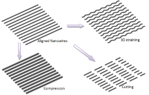
The technique works by using a multilayered sandwich structure that has a tiny mold at the bottom. Nanowires were situated directly above the mold, and other materials were layered between the nanowires and a glass cover sheet. Exposing this layered "forming unit" to an ultra-fast pulsing laser causes one of the layers to burn up, generating a downward pressure that forces the nanowires into the mold and changes their shape.

"The process could be scaled up for an industrial roll-to-roll manufacturing process by changing laser beam size and scanning speed," Cheng said. "The laser shock-induced shaping approach is fast and low-cost."

Part of the research, funded by the National Science Foundation, was carried out in a specialized clean room at the Birck Nanotechnology Center in Purdue's Discovery Park.

Writer: Emil Venere, 765-494-4709, venere@purdue.edu

Source: Gary J. Cheng, 765-494-5436, gjcheng@purdue.edu

Note to Journalists: Copies of the research papers are available by contacting Emil Venere, 765-494-4709, venere@purdue.edu


ABSTRACT

Nanoscale Strainability of Graphene by Laser Shock Induced 3D Shaping

Ji Li 1,2, Ting-Fung Chung 3, Yong P. Chen 1,3,4, Gary J. Cheng *1,2

1 Birck Nanotechnology Center, Purdue University

2 School of Industrial Engineering

3 School of Electrical and Computer Engineering

4 Department of Physics

Graphene has many promising physical properties. It has been discovered that local strain in a graphene sheet can alter its conducting properties and transport gaps. It is of great importance to develop scalable strain engineering techniques to control the local strains in graphene and understand the limit of the strains. Here, we present a scalable manufacturing process to generate 3-D nanostructures and thus induce local strains in the graphene sheet. This process utilizes laser induced shock pressure to generate 3-D tunable straining the graphene sheet. The size dependent straining limit of the graphene and the critical breaking pressure are both studied. It is found that the graphene film can be formed to a circular mold (~50nm in diameter) with an aspect ratio of 0.25 and strain of 12%, and the critical breaking pressure is 1.77GPa. These values were found to be decreasing with the increase of mold size. The local straining and breaking of graphene film are verified by Raman spectra. Large scale processing of the graphene sheet into nano-scale patterns is presented. The process could be scaled up to roll-to-roll process by changing laser beam size and scanning speed. The presented laser shock straining approach is a fast, tunable and low-cost technique to realize strain engineering of graphene for its applications in nano-electrical devices.


ABSTRACT

Laser Shock-Based Platform for Controllable Forming of Nanowires

Ji Li, Yiliang Liao, Sergey Suslov, and Gary J. Cheng*

Birck Nanotechnology Center and School of Industrial Engineering, Purdue University

One-dimensional nanomaterials have attracted a great deal of research interest in the past few decades due to their unique mechanical, electrical and optical properties. Changing the shape of nanowires (NWs) is both challenging and crucial to change the property and open wide functions of NWs, such as strain engineering, electronic transport, mechanical properties, band structure and quantum properties, etc. Here we report a scalable strategy to conduct cutting, bending and periodic straining of NWs by making use of laser shock pressure. Three-dimensional shaping of silver NWs is demonstrated, during which the Ag NWs exhibit very good ductility (strain-to-failure reaches 110%). Meanwhile, the high electrical conductivity of Ag NWs could retain well under controlled laser shock pressure. The microstructure observation indicates that the main deformation mechanism in Ag NWs under dynamic loading is formation of twinning and stacking fault, while dislocation motion and pile-up is less obvious. This method could be applied to semiconductor NWs as well.


Ver artículo...

Archivo del blog